clock

Monday, 24 June 2013

Tenma 72-7740 multimeter: review and teardown

Tenma 72-7740 multimeter: review and teardown

The Tenma 72-7740 digital multimeter is a multimeter in the $70 price range. Overall, it's a nice, solidly-build meter and it has performed well for me. I received this DMM from Newark element14 for review; in this article I describe its functionality followed by a teardown.

What you get

What comes in the box with the Tenma 72-7740 DMM: temperature probe, battery, alligator clips, and probes. The DMM comes with a temperature probe, battery, alligator clips, and test probes. Note that the test probes have very short metal tips, unlike the long tips on most probes. The alligator clip probes are a nice addition. My biggest complaint with the DMM is the temperature probes connections are soldered with no strain relief so I worry the wires will break off.
The DMM also comes with a pocket-sized 36 page operating manual - a real, physical manual on paper, not a PDF file like most products these days. The DMM doesn't really need a manual - functions work pretty much as you'd expect - but it's nice to have the manual.

Specifications

The DMM is autoranging with maximum reading of 3999. It is full-size (177mm × 85mm × 40mm), not a pocket DMM, and has a built-in stand. The LCD display is large and clear and has a backlight, which is nice if I ever end up using the meter in the dark. It has 10MΩ input impedance and maximum voltages of 1000V DC and 750V AC. The top current range is 10A. The DMM also includes capacitance, diode, temperature, frequency, and duty cycle measurements. The top capacitance range (100µF) can take up to 15 seconds to get a measurement, so be patient with those big electrolytics. The lowest capacitance range is 40 nF with 10pF resolution claimed. The DMM also has a continuity buzzer, although I find the sound crackles a bit. The temperature readings are only in °C; I know using Fahrenheit makes me a bad person, but that's what I need to check my appliances. The temperature range is -40°C to 1000°C. The upper range is hotter than I need, but since I sometimes go outside below -40°C my multimeter should be able to handle it too.
Buttons provide hold and relative mode. The meter goes into sleep mode after 30 minutes.
I don't have the equipment to measure the accuracy of the DMM myself, so I'm going off the published values. The specification for DC voltage accuracy is a reasonable ±0.8%; the considerably more expensive Fluke 177 has ±0.09% accuracy, so you get what you pay for.
The function knob has 7 positions: V, resistance/capacitance/diode/continuity, Hertz, °C, µA, mA, and A. The blue function button switches between AC and DC or switches among resistance, capacitance, diode, and continuity.
There are a few functions found in more advanced multimeters that aren't found here: min/max measurement, RS-232 support, °F, a 4nF capacitance scale, and an analog bar graph.
For full specifications, see the specification chart.
Tenma 72-7740 digital multimeter measuring 60Hz line frequency

Teardown

Of course I was interested in what was inside the multimeter and opened it up. The instruction manual describes how to remove the screws under the feet. The force required to pry the case apart made me a little nervous, but it snapped open without breaking anything. Note that the case must also be opened in this way to replace the fuses - they are not accessible from the battery compartment. Unfortunately I tend to blow fuses a lot measuring charger performance, but this may motivate me to be more careful. Inside the Tenma 72-7740 DMM, showing the foil shield, the two fuses, and the thick wire for high-current measurements.
A foil shield covers most of the circuit board, with holes for some adjustments. Near the bottom is a thick wavy wire, which is the precision resistor used for the high-current measurements, a fraction of an ohm. There's nothing particularly interesting directly under the foil shield; almost all the components are on the other side.
Removing the circuit board and flipping it over shows the circuitry. The large LCD display is at the top, with the pushbuttons below. The most visually striking part of the board is the round circuitry for the function knob, which I will explain in more detail below. To the left are three precision (blue) resistors for mA and µA measurement. Below are 5 diodes which I believe are for input protection. The large black cylinder in the lower right appears to be a spark gap to protect the input from high voltages - the DMM is rated to 1000V DC overload protection. Below it is a large yellow PTC resistor to protect from input overloads. The 8-pin IC is a STMicroelectronics TL062C low power J-FET dual op amp.
The circuit board for the Tenma 72-7740 DMM.
Underneath the LCD is the 100-pin controller IC and a bunch of SMD components. The Semico CS7721CN chip powers the Tenma 72-7740 DMM. I wasn't expecting that a DMM chip would need 100 pins, but that seems to be common. I couldn't find a datasheet for this specific chip, but datasheets for other similar chips (such as the Fortune FS9721 and Cyrustek ES51982) give an idea of how digital multimeters works. The chip has signal inputs for the different functions (voltage, current, resistance, frequency, capacitance, etc.) The four blue precision resistors below the chip divide the input by powers of 10 as appropriate. Six mode pins are connected to the function selector switch to select the appropriate function, as will be displayed below. The function pushbuttons are also connected to the IC. About 17 pins from the IC drive the LCD segments. The crystal provides accurate timing, which is critical for the accuracy of the dual-slope analog-to-digital converter that measures the input. The 100-pin Semico CS7721CN chip powers the Tenma 72-7740 DMM.
The 100-pin Semico CS7721CN chip powers the Tenma 72-7740 DMM.

How the function selector switch works

Rotary switches have always been mysterious to me. The pattern on the circuit board seems to be made up of random lines rather than any obvious switch contacts, and looks as much like an Aztec symbol as a switch. So I figured it was time to dive in and figure out how it works. The selector knob has 7 positions, rotating a bit under 180 degrees in total. Looking at the back of the selector knob, you can see six independent sliders for six separate switching circuits. Each slider has two peaks in the middle, which bridge two contacts on the circuit board. Note that the two outermost sliders are offset 90 degrees from the others. Since the knob turns a bit under 180°, the sliders n
The function knob rotates through seven positions and has six independent contacts.
The following diagram shows how the switches work. Each of the six colored semi-circular rings is associated with one of the sliders. The seven lines inside each semicircle indicate the seven possible positions of the associated slider. The most counterclockwise position in each ring is the V setting, followed by Ω, Hz, °C, µA, mA, and A. If there are two traces lined up with the slider, the slider will connect the two traces.
This diagram shows the structure of the function switch on the Tenma 72-7740. Each color shows one of the six independent switches, with lines for the seven possible positions. In highlighted positions, a pair of contacts is closed.
One surprise is that many of the traces don't actually form a circuit. The highlighted positions in the diagram are active positions that close two contacts, but the other positions don't form a connection. In particular, the red ring is only active in one position, and the blue ring in two positions. Many positions have the same circuit trace on both ends of the line, which means the switch does nothing and the trace is unnecessary. My guess is that the redundant metal is there because metal-on-metal is lower friction than metal-on-circuit-board.
The white, cyan, and blue rings ground various combinations of "mode" pins on the IC to select the function. The left half of the purple ring directs the µAmA°C input to the appropriate circuit based on the function. The right half of the purple ring directs the HzVΩ input appropriately. The red ring has a connection only for the °C setting. The orange ring makes connections for Ω, °C, and A.

Conclusion

The 72-7740 DMM is a solid meter that gets the job done and I have only minor complaints. It currently sells for about $70. Inexplicably, the next model up, the 7745, is cheaper despite having true RMS and a serial RS-232 output. The model down, the 7735 is a good deal at about half the price; it also has RS-232, although it lacks temperature measurement, the backlight, and sleep mode. The Tenma 72-7740 DMM in the box.
The Tenma 72-7740 DMM in the box.
Thanks to Newark element14 for giving me this digital multimeter free for review. (Newark element14 consists of the merger of the well-known Newark electronics distributor and the element14 online electronics community into a single global brand.)

overflow flag explained mathematically

The 6502 overflow flag explained mathematically

The overflow flag on the 6502 processor is a source of myth and confusion. In this article, I explain signed and unsigned binary arithmetic, discuss the meaning of the overflow flag, show various formulas for computing overflow, and dispell some myths about the overflow flag.
You might be looking for my other article on overflow - The 6502 CPU's overflow flag explained at the silicon level - which is much more popular.
The 6502 is an 8-bit microprocessor that was very popular in the 1970s and 1980s, powering popular home computers such as the Apple II, Commodore PET, and Atari 400/800. The 6502 instruction set includes 8-bit addition and subtraction operations. Various status flags (carry, zero, negative, overflow) are set based on the result of the operation. Most of the flags (carry, zero, negative) are straightforward, but the meaning of the overflow (V) flag is harder to understand. If the result of a signed add or subtract won't fit into 8 bits, the overflow flag is set. (The overflag is affected in a couple other cases - the BIT operation, and the SO pin on the chip. These are discussed in detail in the excellent article The overflow flag explained, so I won't discuss them here.)

Addition on the 6502

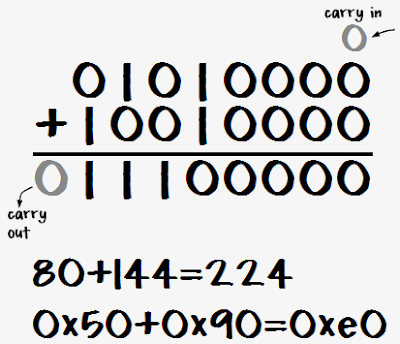
The 6502 has an 8-bit addition operation ADC (add with carry) which adds two numbers and a carry-in bit, yielding an 8-bit result and a carry out bit. The following diagram shows an example addition in binary, decimal, and hexadecimal. Unsigned binary addition of 80 + 44 yielding 224.
The carry flag is used as the carry-in for the operation, and the resulting carry-out value is stored in the carry flag. The carry flag can be used to chain together multiple ADC operations to perform multi-byte addition.

Ones-complement and twos-complement

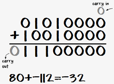
The concepts of ones-complement and twos-complement are important to understand signed arithmetic. The ones complement of a number simply flips all 8 bits in the number. That is, the ones complement of N is 255-N. This is very easy to do in hardware. The twos complement of a number is the ones complement of the number plus 1. That is, the twos complement of N is 256-N. Thw twos complement is very useful because adding M and the twos complement of N is the same as subtracting N from M. For example, to compute 80 - 112, simply take the twos complement of 112 (binary 10010000) and add it to 80 (binary 01010000), yielding (binary 11100000). This result is the twos complement of 32, indicating -32.
Signed binary addition of 80 and -112 yielding -32.
Note that 80+144 and 80-112 had exactly the same bit-level operations - only the interpretation of the bits was different. This is why twos complement numbers are so useful - the same addition circuit works with them.
To see why twos complement numbers work this way, consider M + (-N) or M - N
M - N
→ M - N + 256Adding 256 doesn't change the 8-bit value.
= M + (256 - N)Simple algebra.
= M + twos complement of NDefinition of twos complement.
Thus, adding the twos complement is the same as subtracting. (With the exception of the carry bit, which is affected by the extra 256. This will be discussed later)

Twos-complement signed numbers

Twos complement numbers are very useful for representing signed numbers, since a number between -128 and +127 can fit into one byte: the top bit is 0 for a normal non-negative number (0 to 127), and the top bit is 1 for a twos-complement negative number (-1 to -128). (The value of the top bit is reflected in the N (negative) status flag.) The nice thing about signed numbers is that regular binary arithmetic yields the expected results (in most cases). That is, the processor adds or subtracts the numbers as if they are unsigned binary numbers, and the right answer occurs just by interpreting them as signed.
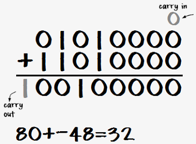
Another example shows that the carry is ignored with signed addition. In this case, 80 and -48 are added, yielding 32. Since 80 + (256-48) = 256 + (80-48), the "extra" 256 ends up in the carry bit.
Signed addition of 80 and -48 yields a carry, which is discarded.
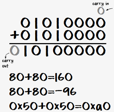
Unfortunately, problems can happen. For instance, 80 + 80 = 160 with unsigned arithmetic, but with signed arithmetic the result is unexpectedly -96. The problem is that 160 will fit into a byte as an unsigned number, but it is too big to store in a byte as a signed number. Since the top bit is set, it is interpreted as a negative number. To indicate this problem, the 6502 sets the overflow flag.
Signed addition of 80 + 80 yields overflow.

The table that explains everything about overflow

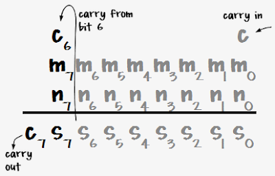
The definition of the 6502 overflow flag is that it is set if the result of a signed addition or subtraction doesn't fit into a signed byte. That is, overflow occurs if the result is > 127 or < -128. The symptom of this is adding two positive numbers and getting a negative result or adding two negative numbers and getting a positive result. This section explores all the possible ways that overflow can occur. The following examples consider the addition of two signed numbers M and N. It is only necessary to consider the top bits of the numbers and the carry from bit 6, as shown in the diagram below, since the lower bits don't affect overflow (except by causing a carry from bit 6).
Binary addition, demonstrating the bits that affect the 6502 overflow flag.
There are 8 possibilities for these bits, as expressed in the table below. For each set of input bits, the table shows the carry out (C7), the top bit of the sum (S7), which is the sign bit, and the overflow bit V. This covers the 4 possibilities for sign of the arguments (positive + positive, positive + negative, negative + positive, negative + negative), with and without carry from bit 6. The table shows an example sum for each line, first expressed in hexadecimal, and then interpreted as unsigned addition and signed addition.
InputsOutputs
Example
M7 N7 C6 C7 S7 VCarry / OverflowHexUnsignedSigned
000000No unsigned carry or signed overflow0x50+0x10=0x6080+16=9680+16=96
001011No unsigned carry but signed overflow0x50+0x50=0xa080+80=16080+80=-96
010010No unsigned carry or signed overflow0x50+0x90=0xe080+144=22480+-112=-32
011100Unsigned carry, but no signed overflow0x50+0xd0=0x12080+208=28880+-48=32
100010No unsigned carry or signed overflow0xd0+0x10=0xe0208+16=224-48+16=-32
101100Unsigned carry but no unsigned overflow0xd0+0x50=0x120208+80=288-48+80=32
110101Unsigned carry and signed overflow0xd0+0x90=0x160208+144=352-48+-112=96
111110Unsigned carry, but no signed overflow0xd0+0xd0=0x1a0208+208=416-48+-48=-96
A few interesting things can be noted from this table. Signed overflow (V=1) happens in two of the eight cases - when the result of adding two positive numbers overflows and ends up negative, and when the result of adding two negative numbers overflows and ends up positive. These rows are highlighted. Signed overflow will never happen when adding a positive number and a negative number, since the result will have a smaller magnitude. Unsigned carry (red in the unsigned column) happens in four of the eight cases, and is independent of signed overflow.

Formulas for the overflow flag

There are several different formulas that can be used to compute the overflow bit. By checking the eight cases in the above table, these formulas can easily be verified. A common definition of overflow is V = C6 xor C7. That is, overflow happens if the carry into bit 7 is different from the carry out.
A second formula simply expresses the two lines that cause overflow: if the sign bits (M7 and N7) are 0 and the carry in is 1, or the sign bits are 1 and the carry in is 0:
V = (!M7&!N7&C6) | (M7&N7&!C6)
The above formula can be manipulated with De Morgan's laws to yield the formula that is actually implemented in the 6502 hardware:
V = not (((m7 nor n7) and c6) nor ((M7 nand N7) nor c6))

Overflow can be computed simply in C++ from the inputs and the result. Overflow occurs if (M^result)&(N^result)&0x80 is nonzero. That is, if the sign of both inputs is different from the sign of the result. (Anding with 0x80 extracts just the sign bit from the result.) Another C++ formula is !((M^N) & 0x80) && ((M^result) & 0x80). This means there is overflow if the inputs do not have different signs and the input sign is different from the output sign (link).

Subtraction on the 6502

The behavior of the overflow flag is fundamentally the same for subtraction, indicating that the result doesn't fit into the signed byte range -128 to 127. The 6502 has a SBC operation (subtract with carry) that subtracts two numbers and also subtracts the borrow bit. If the (unsigned) operation results in a borrow (is negative), then the borrow bit is set. However, there is no explicit borrow flag - instead the complement of the carry flag is used. If the carry flag is 1, then borrow is 0, and if the carry flag is 0, then borrow is 1. This behavior may seem backwards, but note that both for addition and subtraction, if the carry flag is set, the output is one more than if the carry flag is clear. Defining the borrow bit in this way makes the hardware implementation simple. SBC simply takes the ones complement of the second value and then performs an ADC. To see how this works, consider M minus N minus borrow B.
M - N - BSBC of M and N with borrow B
→ M - N - B + 256Add 256, which doesn't change the 8-bit value.
= M - N - (1-C) + 256Replace B with the inverted carry flag.
= M + (255-N) + CSimple algebra.
= M + (ones complement of N) + C255 - N is the same as flipping the bits.
The following table shows the overflow cases for subtraction. It is similar to the previous table, with the addition of the B column that indicates if a borrow resulted. Unsigned operation resulting in borrow are shown in red, as are signed operations that result in an overflow.
InputsOutputs
Example
M7 N7 C6 C7 BS7 VBorrow / OverflowHexUnsignedSigned
0100100Unsigned borrow but no signed overflow0x50-0xf0=0x6080-240=9680--16=96
0110111Unsigned borrow and signed overflow0x50-0xb0=0xa080-176=16080--80=-96
0000110Unsigned borrow but no signed overflow0x50-0x70=0xe080-112=22480-112=-32
0011000No unsigned borrow or signed overflow0x50-0x30=0x12080-48=3280-48=32
1100110Unsigned borrow but no signed overflow0xd0-0xf0=0xe0208-240=224-48--16=-32
1111000No unsigned borrow or unsigned overflow0xd0-0xb0=0x120208-176=32-48--80=32
1001001No unsigned borrow but signed overflow0xd0-0x70=0x160208-112=96-48-112=96
1011010No unsigned borrow or signed overflow0xd0-0x30=0x1a0208-48=160-48-48=-96
Comparing the above table with the overflow table for addition shows the tables are structurally similar if you take the ones-complement of N into account. As with addition, two of the rows result in overflow. However, some things are reversed compared with addition. Overflow can only occur when subtracting a positive number from a negative number or vice versa. Subtracting positive from positive or negative from negative is guaranteed not to overflow.
The formulas for overflow during addition given earlier all work for subtraction, as long as the second argument (N) is ones-complemented. Since internall subtraction is just addition of the ones-complement, N can simply be replaced by 255-N in the formulas.

Overflow myths

There are a lot of myths and confusion about the overflow flag. Since the flag is a bit difficult to understand, simple but wrong explanations are easy to find. The most common myth is that just as the carry bit indicates a carry (or overflow) from bit 7, the overflow bit indicates a carry (or overflow) from bit 6 (example, example, example). As can be seen from the table above, sometimes a carry from bit 6 causes an overflow and sometimes it doesn't.
Another myth is that for multi-byte signed numbers, you use the overflow flag instead of the carry flag to carry from one byte to another (example). In fact, carry is still used to add/subtract multi-byte signed numbers, the same as with unsigned numbers.
It is sometimes claimed that the overflow bit is set if a result is too large to be represented in a byte (example, example). This omits the critical word signed - a signed result can be too large to fit in a byte, even if the unsigned result fits, and vice versa. Examples are in the table above.
Another confusing explanation is that the overflow flag is set when the sign bit is affected (example). The table shows that sometimes there is overflow when the sign bit is affected by bit 6 carry, and sometimes there is overflow when the sign bit is not affected.

Conclusions

This is probably more than anyone really wants to know about the overflow flag. In my next article, I discuss how overflow is implemented at the silicon level.

ECG circuit

A simple ECG circuit which can be implemented using LM741 OP-AMP.

heart beat circuit


Apple didn't revolutionize power supplies ?

Apple didn't revolutionize power supplies; new transistors did

The new biography Steve Jobs contains a remarkable claim about the power supply of the Apple II and its designer Rod Holt:[1]
Instead of a conventional linear power supply, Holt built one like those used in oscilloscopes. It switched the power on and off not sixty times per second, but thousands of times; this allowed it to store the power for far less time, and thus throw off less heat. "That switching power supply was as revolutionary as the Apple II logic board was," Jobs later said. "Rod doesn't get a lot of credit for this in the history books but he should. Every computer now uses switching power supplies, and they all rip off Rod Holt's design."
I found it amazing to think that computers now use power supplies based on the Apple II's design, so I did some investigation. It turns out that Apple's power supply was not revolutionary, either in the concept of using a switching power supply for computers or in the specific design of the power supply. Modern computer power supplies are totally different and do not rip off anything from Rod Holt's design. It turns out that Steve Jobs was making his customary claim that everyone is stealing Apple's revolutionary technology, entirely contrary to the facts. The history of switching power supplies turns out to be pretty interesting. While most people view the power supply as a boring metal box, there's actually a lot of technological development behind it. There was, in fact, a revolution in power supplies in the late 1960s through the mid 1970s as switching power supplies took over from simple but inefficient linear power supplies, but this was a few years before the Apple II came out in 1977. The credit for this revolution should go to advances in semiconductor technology, specifically improvements in switching transistors, and then innovative ICs to control switching power supplies.[2]

Some background on power supplies

In a standard desktop computer, the power supply converts AC line voltage into DC, providing several carefully regulated low voltages at high currents. Power supplies can be built in a variety of ways, but linear and switching power supplies are the two techniques relevant to this discussion. (See the notes for more about obsolete technologies such as large mechanical motor-generator systems[3] and ferroresonant transformers[4][5].) A typical linear power supply uses a bulky power transformer to convert the 120V AC into a low AC voltage, converts this to low voltage DC with a diode bridge, and then uses a linear regulator to drop the voltage to the desired level. The linear regulator is an inexpensive easy-to-use transistor-based component that turns the excess voltage into waste heat to produce a stable output. Linear power supplies are almost trivial to design and build.[6] One big disadvantage however, is they typically waste about 50-65% of the power as heat,[7] often requiring large metal heat sinks or fans to get rid of the heat. The second disadvantage is they are large and heavy. On the plus side, the components (other than the transformer) in linear power supplies only need to handle low voltages and the output is very stable and noise-free.
A switching power supply works on a very different principle: rapidly turning the power on and off, rather than turning excess power into heat. In a switching power supply, the AC line input is converted to high-voltage DC, and then the power supply switches the DC on and off thousands of times a second, carefully controlling the time of the switching so the output voltage averages out to the desired value. Theoretically, no power gets wasted, although in practice the efficiency will be 80%-90%. Switching power supplies are much more efficient, give off much less heat, and are much smaller and lighter than linear power supplies. The main disadvantage of a switching power supply is it is considerably more complex than a linear power supply and much harder to design.[8] In addition, it is much more demanding on the components, requiring transistors that can efficiently switch on and off at high speed under high power. The switches, inductors, and capacitors in a switching power supply can be arranged in several different arrangements (or topologies), with names such as Buck, Boost, Flyback, Forward, Push-Pull, Half Wave, and Full-Wave.[9]

History of switching power supplies to 1977

Switching power supply principles were known since the 1930s[6] and were being built out of discrete components in the 1950s.[10] In 1958, the IBM 704 computer used a primitive vacuum-tube based switching regulator.[11] The company Pioneer Magnetics started building switching power supplies in 1958[12] (and decades later made a key innovation in PC power supplies[13]). General Electric published an early switching power supply design in 1959.[14] In the 1960s the aerospace industry and NASA[15] were the main driving force behind switching power supply development, since the advantages of small size and high efficiency made up for the high cost.[16] For example, NASA used switching supplies for satellites[17][18] such as Telstar in 1962.[19] The computer industry started using switching power supplies in the late 1960s and they steadily grew in popularity. Examples include the PDP-11/20 minicomputer in 1969,[20] the Honeywell H316R in 1970,[21] and Hewlett-Packard's 2100A minicomputer in 1971.[22][23] By 1971, companies using switching regulators "read like a 'Who's Who' of the computer industry: IBM, Honeywell, Univac, DEC, Burroughs, and RCA, to name a few."[21] In 1974, HP used a switching power supply for the 21MX minicomputer,[24] Data General for the Nova 2/4,[25] Texas Instruments for the 960B,[26] and Interdata for their minicomputers.[27] In 1975, HP used an off-line switching power supply in the HP2640A display terminal,[28] Matsushita for their traffic control minicomputer,[29] and IBM for its typewriter-like Selectric Composer[29] and for the IBM 5100 portable computer.[30] By 1976, Data General was using switching supplies for half their systems, Hitachi and Ferranti were using them,[29] Hewlett-Packard's 9825A Desktop Computer[31] and 9815A Calculator[32] used them, and the decsystem 20[33] used a large switching power supply. By 1976, switching power supplies were showing up in living rooms, powering color television receivers.[34][35]
Switching power supplies also became popular products for power supply manufacturers starting in the late 1960s. In 1967, RO Associates introduced the first 20Khz switching power supply product,[36] which they claim was also the first switching power supply to be commercially successful.[37] NEMIC started developing standardized switching power supplies in Japan in 1970.[38] By 1972, most power supply manufacturers were offering switching power supplies or were about to offer them.[5][39][40][41][42] HP sold a line of 300W switching power supplies in 1973,[43] and a compact 500W switching power supply[44] and a 110W fanless switching power supply[45] in 1975. By 1975, switching power supplies were 8% of the power supply market and growing rapidly, driven by improved components and the desire for smaller power supplies for products such as microcomputers.[46]
Switching power supplies were featured in electronics magazines of this era, both in advertisements and articles. Electronic Design recommended switching power supplies in 1964 for better efficiency.[47] The October 1971 cover of Electronics World featured a 500W switching power supply and an article "The Switching Regulator Power Supply". A long article about power supplies in Computer Design in 1972 discussed switching power supplies in detail and the increasing use of switching power supplies in computers, although it mentions some companies were still skeptical about switching power supplies.[5] In 1973, Electronic Engineering featured a detailed article "Switching power supplies: why and how".[42] In 1976, the cover of Electronic Design[48] was titled "Suddenly it's easier to switch" describing the new switching power supply controller ICs, Electronics ran a long article on switching power supplies,[29] Powertec ran two-page ads on the advantages of their switching power supplies with the catchphrase "The big switch is to switchers",[49] and Byte magazine announced Boschert's switching power supplies for microcomputers.[50]
A key developer of switching power supplies was Robert Boschert, who quit his job and started building power supplies on his kitchen table in 1970.[51] He focused on simplifying switching power supplies to make them cost-competitive with linear power supplies, and by 1974 he was producing low-cost power supplies in volume for printers,[51][52] which was followed by a a low-cost 80W switching power supply in 1976.[50] By 1977 Boschert Inc had grown to a 650-person company[51] that producing power supplies for satellites and the F-14 fighter aircraft,[53] followed by power supplies for companies such as HP[54] and Sun. People often think of the present as a unique time for technology startups, but Boschert illustrates that kitchen-table startups were happening even 40 years ago.
The advance of the switching power supply during the 1970s was largely driven by new components.[55] The voltage rating of switching transistors was often the limiting factor,[5] so the introduction of high voltage, high speed, high power transistors at a low cost in the late 1960s and early 1970s greatly increased the popularity of switching power supplies.[5][6][21][16] Transistor technology moved so fast that a 500W commercial power supply featured on the cover of Electronics World in 1971 couldn't have been built with the transistors of just 18 months earlier.[21] Once power transistors could handle hundreds of volts, power supplies could eliminate the heavy 60 Hz power transformer and run "off-line" directly from line voltage. Faster transistor switching speeds allowed more efficient and much smaller power supplies. The introduction of integrated circuits to control switching power supplies in 1976 is widely viewed as ushering in the age of switching power supplies by drastically simplifying them.[10][56]
By the early 1970s, it was clear that a revolution was taking place. Power supply manufacturer Walt Hirschberg claimed in 1973 that "The revolution in power supply design now under way will not be complete until the 60-Hz transformer has been almost entirely replaced."[57] In 1977, an influential power supply book said that "switching regulators were viewed as in the process of revolutionizing the power supply industry".[58]

The Apple II and its power supply

The Apple II personal computer was introduced in 1977. One of its features was a compact, fanless switching power supply, which provided 38W of power at 5, 12, -5, and -12 volts. Holt's Apple II power supply uses a very simple design, with an off-line flyback converter topology.[59] Steve Jobs said that every computer now rips off Rod Holt's revolutionary design.[1] But is this design revolutionary? Was it ripped off by every other computer?
As illustrated above, switching power supplies were in use by many computers by the time the Apple II was released. The design is not particularly revolutionary, as similar simple off-line flyback converters were being sold by Boschert[50][60] and other companies. In the long term, building the control circuitry out of discrete components as Apple did was a dead-end technology, since the future of switching power supplies was in PWM controller ICs.[2] It's surprising Apple continued using discrete oscillators in power supplies even through the Macintosh Classic, since IC controllers were introduced in 1975.[48] Apple did switch to IC controllers, for instance in the Performa[61] and iMacs.[62]
The power supply that Rod Holt designed for Apple was innovative enough to get a patent,[63] so I examined the patent in detail to see if there were any less-obvious revolutionary features. The patent describes two mechanisms to protect the power supply against faults. The first (claim 1) is a mechanism to safely start the oscillator through an AC input. The second mechanism (claim 8) returns excess energy from the transformer to the power source (especially if there is no load) through a clamp winding on the transformer and a diode.
Apple II power supply
This is the AA11040-B power supply for the Apple II Plus.[59] AC power enters, on the left, is filtered, goes through the large switching transistor to the flyback transformer in the middle, is rectified by the diodes to the right (on heatsinks), and then is filtered by the capacitors on the right. The control circuitry is along the bottom. Photo used by permission from kjfloop, Copyright 2007.
The AC start mechanism was not used by the Apple II,[59] but was used by the Apple II Plus,[64] Apple III,[65] Lisa,[66] Macintosh,[67] and Mac 128K through Classic.[68] I could not find any non-Apple power supplies that use this mechanism,[69] except for a 1978 TV power supply,[70] and it became obsoleted by IC controllers, so this mechanism seems to have had no impact on computer power supply design.
The second mechanism in Holt's patent, the clamp winding and diode to return power in a flyback converter, was used in a variety of power supplies until the mid-1980s and then disappeared. Some examples are the Boschert OL25 power supply (1978),[60] Apple III (1980),[65] Apple's power supply documentation (1982),[59] Tandy hard drive (1982),[71] Tandy 2000 (1983),[72][73] Apple Lisa (1983),[66] Apple Macintosh (1984),[67] Commodore Model B128 (1984),[74] Tandy 6000 (1985),[75] and Mac Plus (1986) to Mac Classic (1990).[68] This flyback clamp winding seems to have been popular with Motorola in the 1980s, appearing in the MC34060 controller IC datasheet,[76] a 1983 designer's guide[77] (where the winding was described as common but optional), and a 1984 application note.[78]
Is this flyback clamp winding the innovation of Holt's that other companies ripped off? I thought so, until I found a 1976 power supply book that described this winding in detail,[35] which ruined my narrative. (Also note that forward converters (as opposed to flyback converters) had used this clamp winding dating back to 1956,[79][80][81] so applying it to a flyback converter doesn't seem like a huge leap in any case.)
One puzzling aspect of power supply discussion in the book Steve Jobs[1] is the statement that the Apple II's power supply is "like those used in oscilloscopes", since oscilloscopes are just one small use for switching power supplies. This statement apparently arose because Holt had previously designed a switching power supply for oscilloscopes,[82] but there's no other connection between Apple's power supply and oscilloscope power supplies.
The biggest impact of the Apple II on the power supply industry was on Astec - the Hong Kong company that manufactured the power supply. Before the Apple II came out, Astec was a little-known manufacturer, selling switching DC-DC inverters. But by 1982, Astec had become the world's top switching-powers-supply manufacturer, almost entirely based on Apple's business, and kept the top spot for a number of years.[83][84] In 1999, Astec was acquired by Emerson,[85] which is currently the second-largest power supply company after Delta Electronics.[86]
A little-known fact about the Apple II power supply is that it was originally assembled by middle-class California housewives as piecework.[83] As demand grew, however, power supply construction was transferred to Astec, even though it cost $7 a unit more. Astec was building 30,000 Apple power supplies monthly by 1983.[83]

Power supplies post-Apple

In 1981, the IBM PC was launched, which would have lasting impact on computer power supply designs. The power supply for the original IBM 5150 PC was produced by Astec and Zenith.[83] This 63.5W power supply used a flyback design controlled by a NE5560 power supply controller IC.[87] I will compare the IBM 5150 PC power supply with the Apple II power supply in detail to show their commonalities and differences. They are both off-line flyback power supplies with multiple outputs, but that's about all they have in common. Even though the PC power supply uses an IC controller and the Apple II uses discrete components, the PC power supply uses approximately twice as many components as the Apple II power supply. While the Apple II power supply uses a variable frequency oscillator built out of transistors, the PC power supply uses a fixed-frequency PWM oscillator provided by the NE5560 controller IC. The PC uses optoisolators to provide voltage feedback to the controller, while the Apple II uses a small transformer. The Apple II drives the power transistor directly, while the PC uses a drive transformer. The PC checks all four power outputs against lower and upper voltage limits to make sure the power is good, and shuts down the controller if any voltages are out of spec. The Apple II instead uses a SCR crowbar across the 12V output if that voltage is too high. While the PC flyback transformer has a single primary winding, the Apple II uses an extra primary clamp winding to return power, as well as an another primary winding for feedback. The PC provides linear regulation on the 12V and -5V supplies, while the Apple II doesn't. The PC uses a fan, while the Apple II famously doesn't. It's clear that the IBM 5150 power supply does not "rip off" the Apple II power supply design, as they have almost nothing in common. And later power supply designs became even more different.
The IBM PC AT power supply became a de facto standard for computer power supplies. In 1995, Intel introduced the ATX motherboard specification,[88] and the ATX power supply (along with variants) has become the standard for desktop computer power supplies, with components and designs often targeted specifically at the ATX market.[89]
Computer power systems became more complicated with the introduction of the voltage regulator module (VRM) in 1995 for the Pentium Pro, which required lower voltage at higher current than the power supply could provide directly. To supply this power, Intel introduced the VRM - a DC-DC switching regulator installed next to the processor that reduces the 12 volts from the power supply to the low voltage used by the processor.[90] (If you overclock your computer, it is the VRM that lets you raise the voltage.) In addition, graphics cards can have their own VRM to power a high-performance graphics chip. A fast processor can require 130 watts from the VRM. Comparing this to the half watt of power used by the Apple II's 6502 processor[91] shows the huge growth in power consumption by modern processors. A modern processor chip alone can use more than twice the power of the whole IBM 5150 PC or three times that of the Apple II.
The amazing growth of the computer industry has caused the power consumption of computers to be a cause for environmental concern, resulting in initiatives and regulations to make power supplies more efficient.[92] In the US, Energy Star and 80 PLUS certification[93] pushes manufacturers to manufacture more efficient "green" power supplies. These power supplies squeeze out more efficiency through a variety of techniques: more efficient standby power, more efficient startup circuits, resonant circuits (also known as soft-switching and ZCT or ZVT) that reduce power losses in the switching transistors by ensuring that no power is flowing through them when they turn off, and "active clamp" circuits to replace switching diodes with more efficient transistor circuits.[94] Improvements in MOSFET transistor and high-voltage silicon rectifier technology in the past decade has also led to efficiency improvements.[92]
Power supplies can use the AC line power more efficiently through the technique of power factor correction (PFC).[95] Active power factor correction adds another switching circuit in front of the main power supply circuit. A special PFC controller IC switches this at a frequency of up to 250kHZ, carefully extracting a smooth amount of power from the power supply to produce high-voltage DC, which is then fed into a regular switching power supply circuit.[13][96] PFC also illustrates how power supplies have turned into a commodity with razor-thin margins, where a dollar is a lot of money. Active power factor correction is considered a feature of high-end power supplies, but its actual cost is only about $1.50.[97]
Many different controller chips, designs, and topologies have been used for IBM PC power supplies over the years, both to support different power levels, and to take advantage of new technologies.[98] Controller chips such as the NE5560 and SG3524 were popular in early IBM PCs.[99] The TL494 chip became very popular in a half-bridge configuration,[99] the most popular design in the 1990s.[100] The UC3842 series was also popular for forward converter configurations.[99] The push for higher efficiency has made double forward converters more popular,[101] and power factor correction (PFC) has made the CM6800 controller very popular,[102] since the one chip controls both circuits. Recently, forward converters that generate only 12V have become more common, using DC-DC converters to produce very stable 3.3V and 5V outputs.[94] More detailed information on modern power supplies is available from many sources.[103][104][98][105]
XT power supply
This typical 150W XT power supply uses the popular half-bridge design. The AC input filtering is on the right. To the left of this is the control/driver ciruit: the TL494 IC at the top controls the small yellow drive transfomer below, which drives the two switching transistors on the heatsinks below. To the left of this is the larger yellow main transformer, with the secondary diodes and regulator on the heatsinks, and output filtering to the left. This half-bridge power supply design is totally different from the Apple II's flyback design. Photo copyright larrymoencurly, used with permission.
Modern computers contain a surprising collection of switching power supplies and regulators. A modern power supply can contain a switching PFC circuit, a switching flyback power supply for standby power, a switching forward converter to generate 12 volts, a switching DC-DC converter to generate 5 volts, and a switching DC-DC converter to generate 3.3 volts,[94] so the ATX power supply can be considered five different switching power supplies in one box. In addition, the motherboard has a switching VRM regulator to power the processor, and the graphics card has another VRM, for a total of seven switching supplies in a typical desktop computer.
The technology of switching power supplies continues to advance. One development is digital control and digital power management.[106] Instead of using analog control circuits, digital controller chips digitize the control inputs and use software algorithms to control the outputs. Thus, designing the power supply controller becomes as much a matter of programming as of hardware design. Digital power management lets power supplies communicate with the rest of the system for higher efficiency and logging. While these digital technologies are largely used for servers now, I expect they will trickle down to desktop computers eventually.
To summarize, the original IBM 5150 PC power supply was different in almost every way from the Apple II power supply, except both were flyback power supplies. More recent power supplies don't even have that in common with the Apple II. It's absurd to claim that power supplies are ripping off Apple's design.

Famous switching power supply designers

Steve Jobs said that Rod Holt should be better known for designing the Apple II's power supply: "Rod doesn't get a lot of credit for this in the history books but he should."[1] But even at best, power supply designers aren't famous outside a very small community. Robert Boschert was inducted into Electronic Design's Electronic Engineering Hall of Fame in 2009 for his power supply work.[51] Robert Mammano got Power Electronics Technology's lifetime achievement award in 2005 for starting the PWM controller IC industry.[10] Rudy Severns got Power Electronics Technology's lifetime achievement award in 2008 for his innovations in switching power supplies.[107] But none of these people are even Wikipedia-famous. Other major innovators in the field get even less attention.[108] I repeatedly came across the work of Elliot Josephson, who designed satellite power systems in the early 1960s[18], has a bunch of power supply patents including the Tandy 6000[75], and even has his patent number printed on the Apple II Plus and Osborne 1 power supply circuit boards[59], but he appears to be entirely unrecognized. The irony in Steve Jobs' comment that Rod Holt doesn't get a lot of credit is that Rod Holt's work is described in dozens of books and articles about Apple, from Revenge of the Nerds in 1982[109] to 2011's best-selling Steve Jobs biography, which makes Rod Holt easily the most famous power supply designer ever.

Conclusion

Power supplies aren't the boring metal boxes that most people think; they have a lot of interesting history, driven largely by the improvements in transistors that made switching power supplies practical for computers in the early 1970s. More recently, efficiency standards such as 80 PLUS have forced power supplies to become more efficient, resulting in new designs. The Apple II sold a huge number of switching power supplies, but its power supply design was a technological dead end that was not "ripped off" by other computers. If you're interested in power supplies, you might also like my article Tiny, cheap, and dangerous: Inside a (fake) iPhone charger.

Saturday, 25 May 2013

Where USB Memory Sticks are Born?

Where USB Memory Sticks are Born

In January, I had the fortune of being a keynote speaker at LCA2013. One of the tchotchkes I received from the conference organizers was a little USB memory stick.


I thought it was a neat coincidence that I was in a factory that manufactured exactly such memory sticks about a week before the conference. In fact, I managed to score a rare treat: the factory owner gave me a sheet of raw chip-on-flex, prior to bonding and encapsulation, to take home.
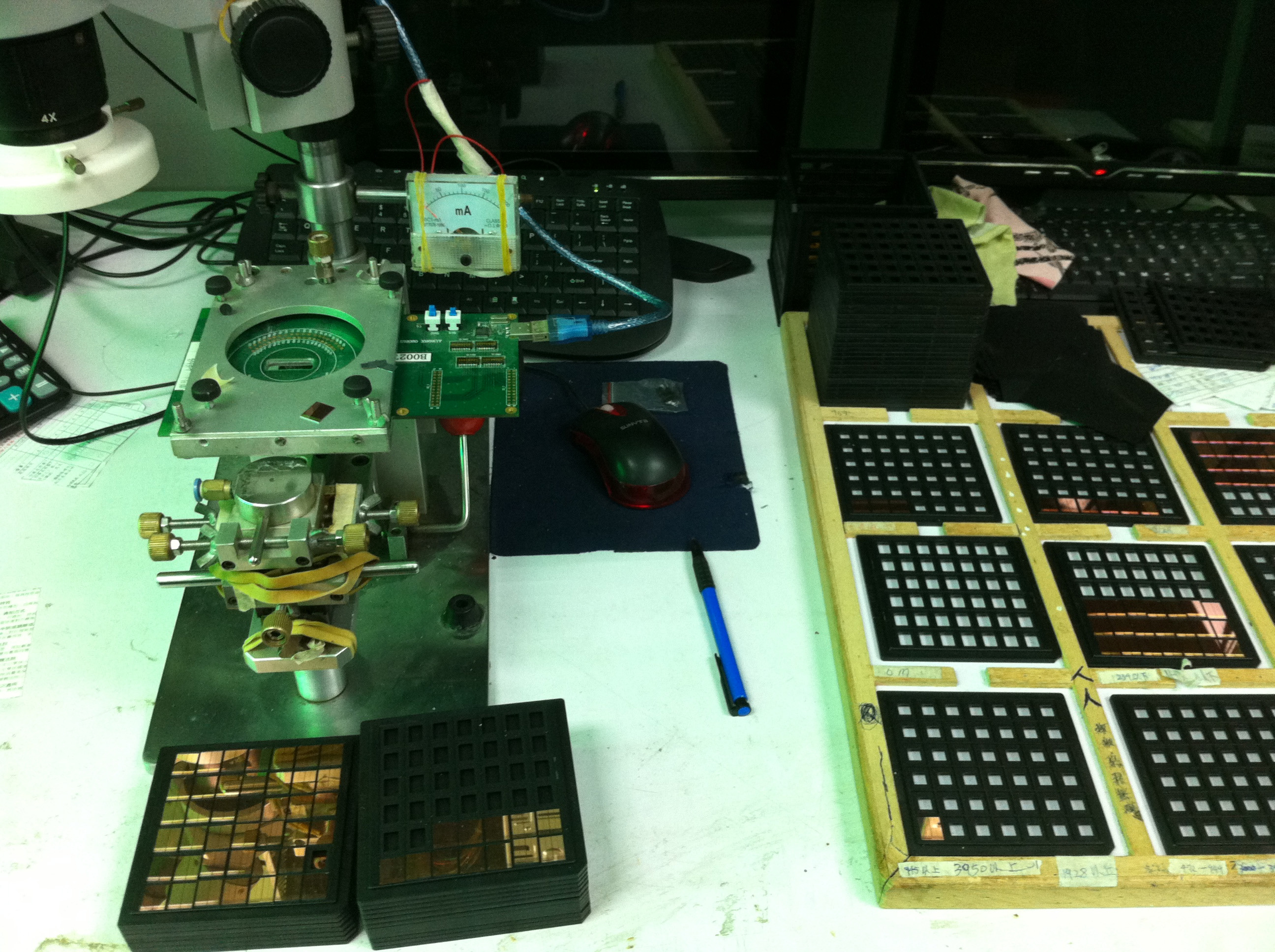
The USB sticks start life as bare FLASH memory chips. Prior to mounting on PCBs, the chips are screened for capacity and functionality. Below is a photo of the workstation where this happens:

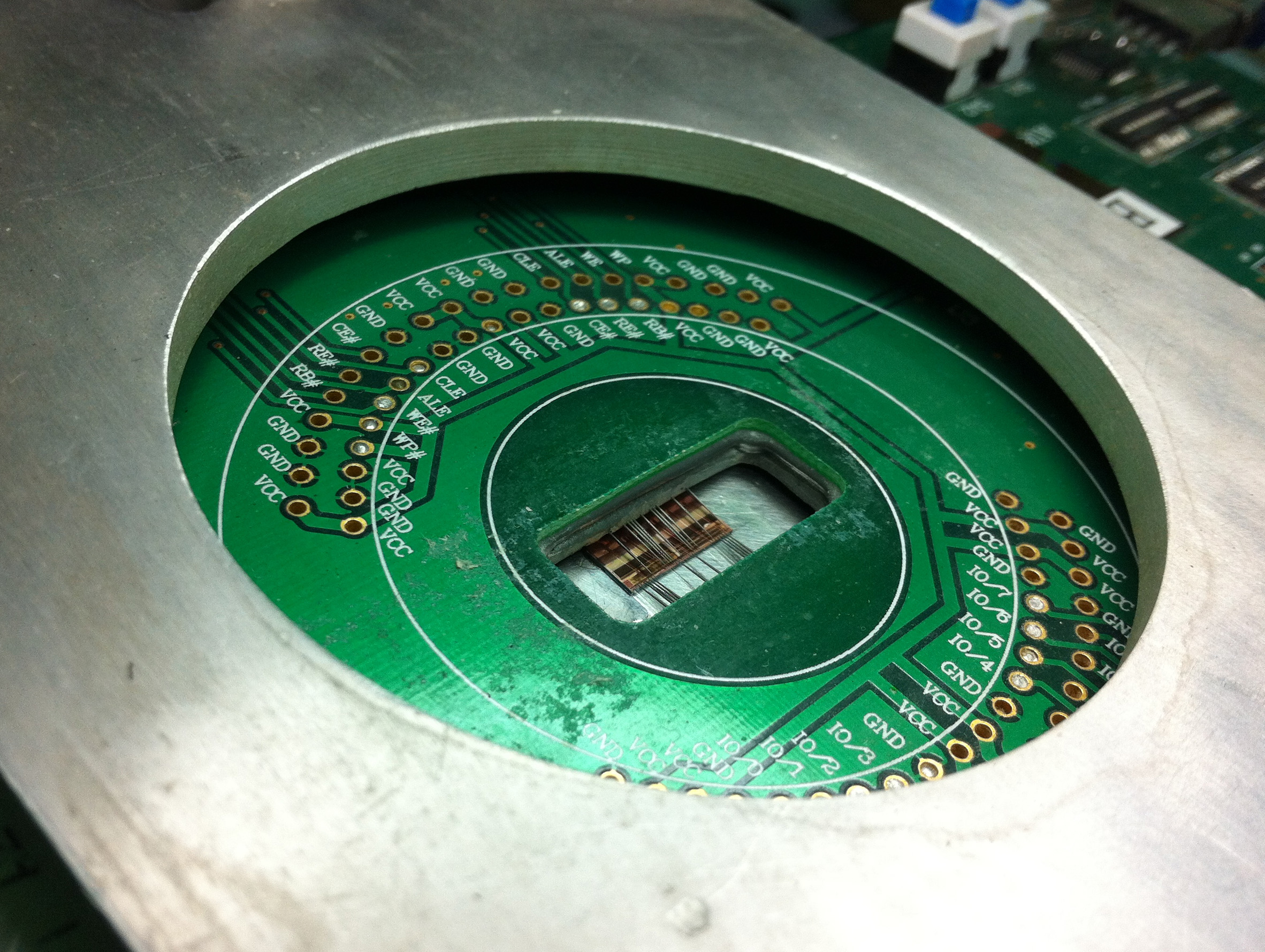
In the image, you can see stacks of bare-die FLASH chips, awaiting screening with a probe card. I love the analog current meter and the use of rubber bands to hold it all together. The probe card has tiny needles on it that touch down on microscopic (less than 100-micron square) contacts on the chip surfaces. Below is what a probe card looks like.

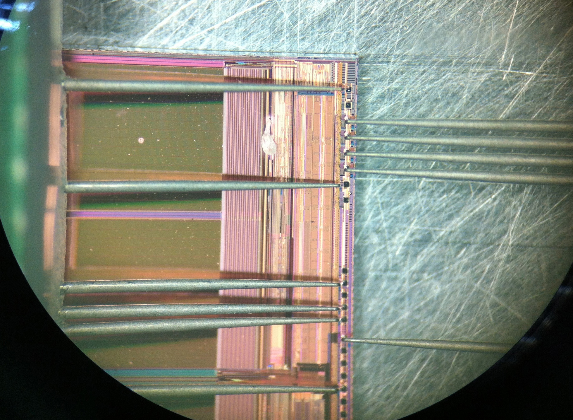
Below is an image through the microscope on the micro-probing station, showing the needles touching down on the square pads at the edge of the FLASH chip’s surface.

Interestingly, this all happens in an absolutely non-clean-room environment. Workers are pretty much handling chips with tweezers and hand suction vises, and mounting the devices into these jigs by hand.
Once the chips are screened for functionality, they are placed by hand onto a PCB. This is not an unusual practice, pretty much every value-oriented wirebonding facility I’ve visited relies on the manual placement of bare die. The photo below shows a controller IC being placed on a panel of PCBs. The bare die are in the right hand side of the photo, sitting in the beige colored waffle pack.

The lady is using some sort of tool made out of hand-cut bamboo. I still haven’t figured out exactly how they work, but every time I’ve seen this process they are using what looks like a modified chopstick to place the chips on the board. My best guess is that the bamboo sticks have just the right surface energy to adhere to the silicon die, such that silicon will stick to the tip of the bamboo rod. A dot of glue is pre-applied to the bare boards, so when the operator touches the die down onto the glue, the surface tension of the glue pulls the die off of the bamboo stick.
It’s trippy to think that the chips inside my USB stick were handled using modified chopsticks.

The chips are then wirebonded to the board using an automated bonding machine which uses image recognition to find the location of the bond pads (this is part of the reason they can get away with manual die placement).
(view in HD)
The first half of the video above starts out with the operator pulling off and replacing a mis-bonded wire by hand, and re-feeding the wire into the machine. Given that these wires are thinner than a strand of hair, and that the bonding pads are microscopic, this is no mean feat of manual dexterity.
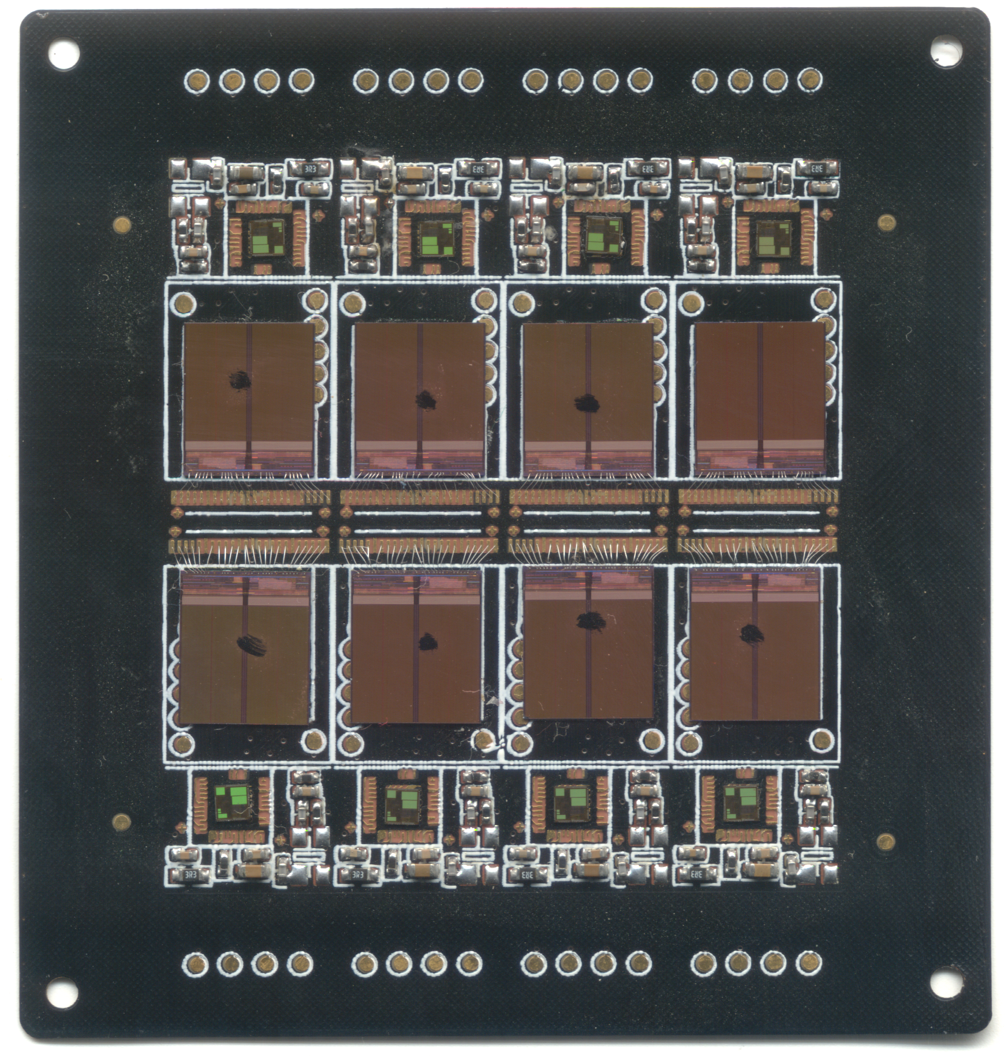
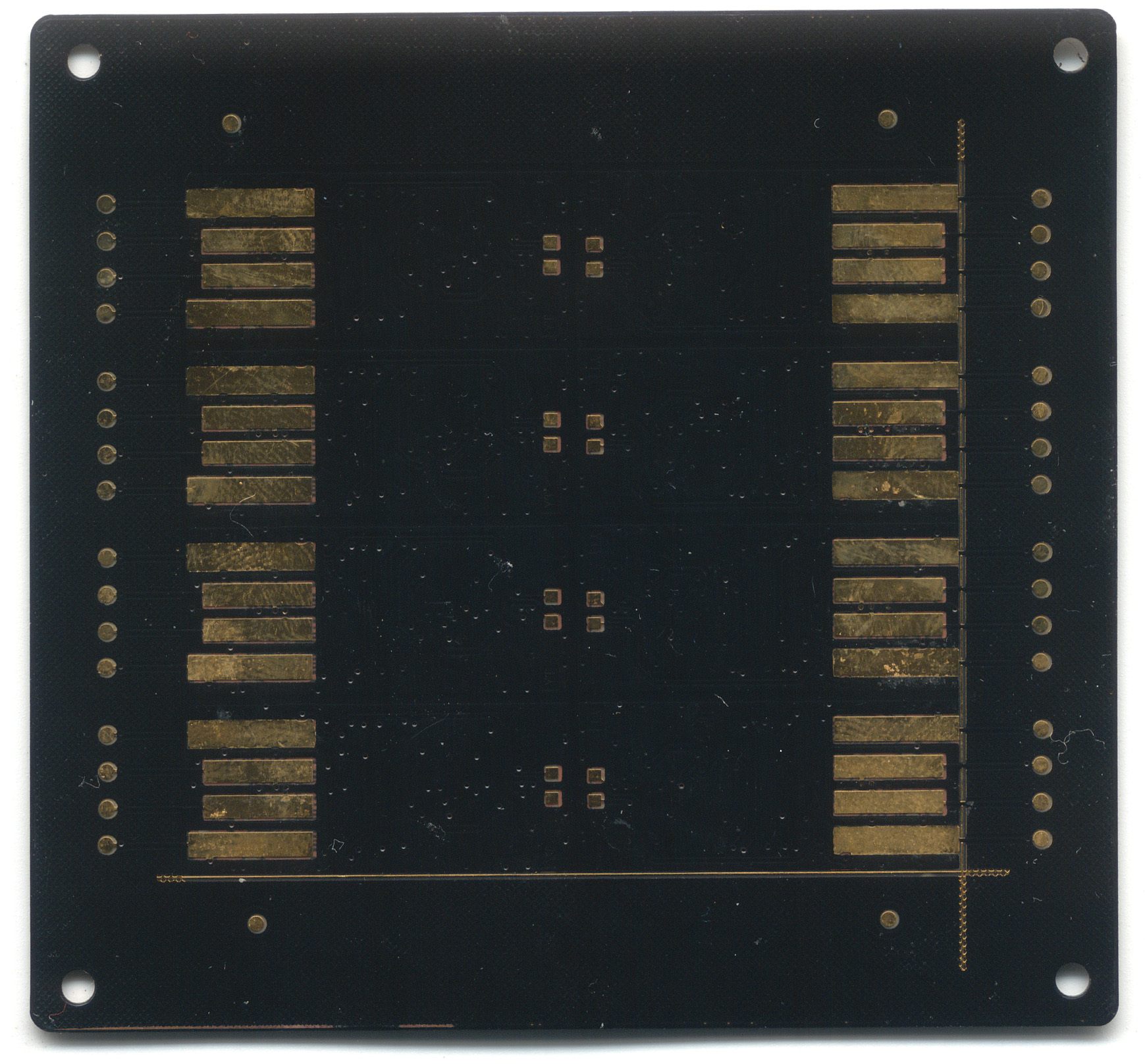
Here’s a scan of the partially-bonded but fully die-mounted PCB that I was given as a memoir from my visit (I had since crushed some of the wire bonds). The panel contains eight USB sticks, each consisting of a FLASH memory chip and a controller IC that handles the bridging between USB and raw FLASH, a non-trivial task that includes managing bad block maps and error-correction, among other things. The controller is probably an 8051-class CPU running at a few dozen MHz.


Once the panels are bonded and tested, they are overmolded with epoxy, and then cut into individual pieces, ready for sale.
Interestingly, the entire assembly prior to encapsulation is flexible. The silicon chips have been thinned down by grinding off their back sides to the point where they can tolerate a small amount of flexing, and the PCB is also so thin, it is flexible.

For those of you interested in this kind of thing, here’s the die marking from the FLASH chip; apparently it is made by Intel:

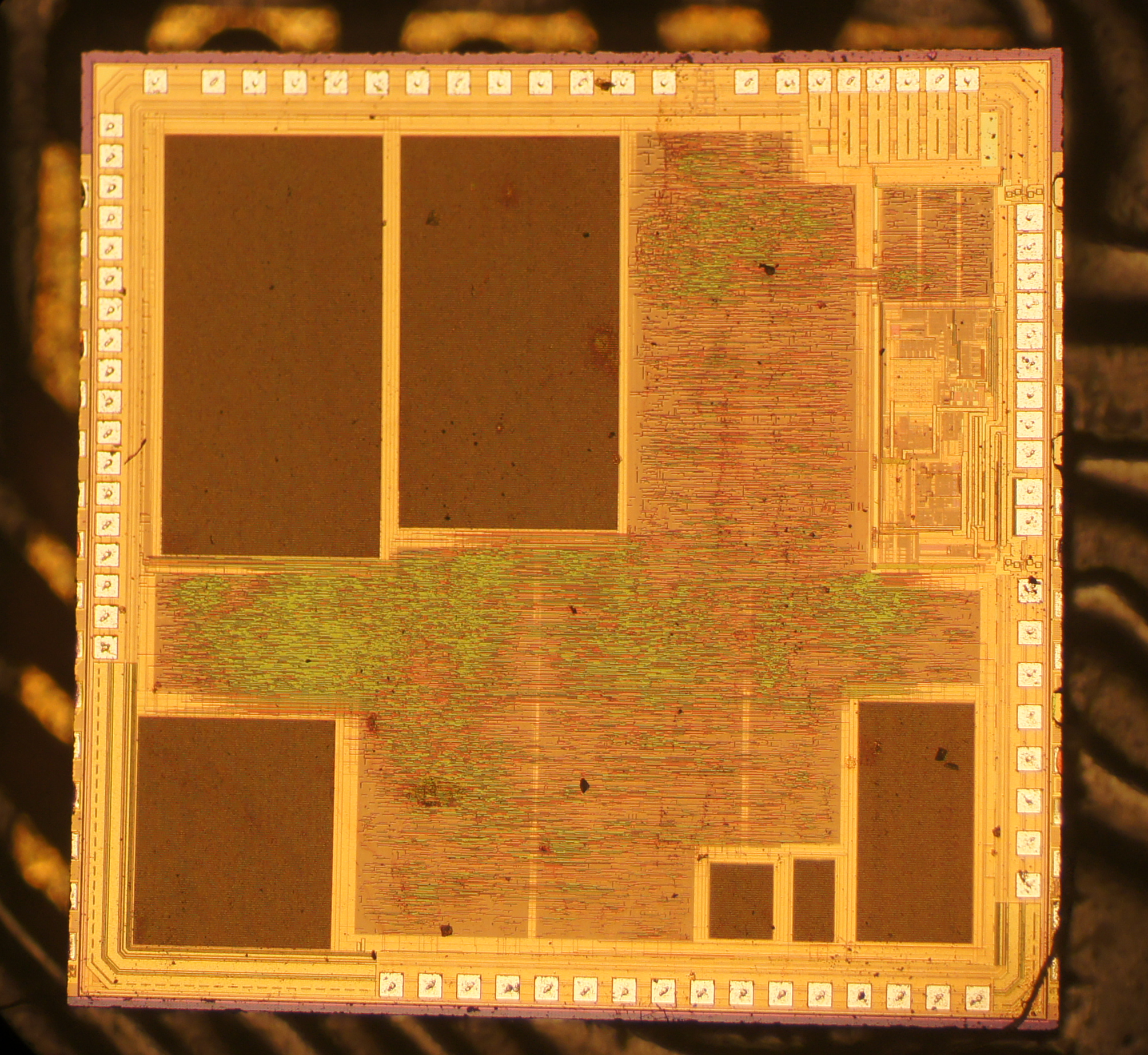
Here is also a die shot of the controller chip:

And now you know where those tiny USB thumb drives are born.
Thanks to David Cranor for contributing images. Images used with permission.
PS: chopsticks

A Simple SMS Based Controlling Different Industrial Machines Using GSM Mobile and microcontroller 8051

A simple SMS Based Controlling Machines Using GSM Mobile and microcontroller 8051

SMS Based Controlling Different Industrial Machines Using GSM Mobile and microcontroller 8051
This project (interfacing mobile phone with microcontroller 8051 for machines control through SMS) has many important other applications and can be used to control Switch ON or OFF any machines at far off places using a gsm modem by sending sms through the communication between the mobile and the embedded devices (microcontroller 8051).This remote control of appliances is possible through Embedded Systems. The use of “Embedded System in Communication” has given rise to many interesting applications that ensures comfort and safety to human life. The microcontroller is interfaced with GSM Modem in mobile phone via MAX232 level convertor. The microcontroller project is designed to allow easy use of a mobile phone to control appliances or machines at any far location may be in industry or at home. Using a mobile phone the development of the control system will be carried out using SMS. This will communicate with another mobile phone, which in turn controls the devices attached to microcontroller modules. moving message display using 8051 microcontroller When the action has been carried out then a response is sent to the user. The use of mobile phones to remotely control an appliance control system. The microcontroller would then control the device based on the information given to it.This post also relates to the project of microcontroller interfacing with lcd and gsm to display the msg sent to interfaced gsm,sms based on off control of a motor throgh 8051 micro controller ,methodology of designing a gsm base noticeboard and motor control through sms circuit diagram .

The devices are connected to the 8051 microcontroller using relays and optocouplers. These relay are controlled through software to switch ON or OFF the device as required. For every message received to microcontroller through mobile phone in form of SMS, the controller will check for the valid and pre-define formate. If the message is correct the controller will perform the operation. microcontroller interfacing with lcd and gsm to display the msg sent to interfaced gsm

The hardware board contains microcontroller AT89c52 at the heart of the system. The microcontroller is interfaced with GSM Modem of mobile phone via MAX232 level convertor. It is used to convert RS232 voltage levels to TTL voltage levels. display the message in notice board with the help of mobile 8051 project gsm architecture based motor on and off circuit diagram

The AT89C52 is a low-power, high-performance CMOS 8-bit microcomputer with 8K bytes of Flash programmable and erasable read only memory (PEROM). The device is compatible with the industry-standard 80C51 and 80C52 instruction set and pin out. The on-chip Flash allows the program memory to be reprogrammed in-system or by a conventional non-volatile memory programmer which provides a highly-flexible and cost-effective solution to many embedded control applications.A GSM modem is a wireless modem that works with a GSM wireless network. A wireless modem behaves like a dial-up modem. The main difference between them is that a dial-up modem sends and receives data through a fixed telephone line while a wireless modem sends and receives data through radio waves. Like a GSM mobile phone, a GSM modem requires a SIM card from a wireless carrier in order to operate.controlling machines using gsm mobile sms services
Generally, computers use AT commands to control modems. Reading of message from the SIM card inserted into the modem is done by sending the appropriate AT command to the modem.
The MAX232 is a dual driver/receiver that includes a capacitive voltage generator to supply EIA-232 voltage levels from a single 5-V supply. Each receiver converts EIA- 232 inputs to 5-V TTL/CMOS levels. Each driver converts TTL/CMOS input levels into EIA-232 levels.
SMS Based Controlling Machines Using GSM Mobile and microcontroller 8051 tutorial tracker gps gsm


GSM Modem, which works at RS-232 voltage levels, logic 1 varies from -3 to -15 volts and logic 0 from +3 to +15 volts. The microcontroller which works on TTL logic levels, logic 1 is +5 volts and logic 0 is 0 volts. Therefore to interface the two we use a MAX 232 driver IC.tutorial tracker gps gsm


AT-Command set
The following section describes the AT-Command set. The commands can be tried out by connecting a GSM modem to one of the PC’s COM ports. Type in the test-command, adding CR + LF (Carriage return + Line feed = \r\n) before executing. Table gives an overview of the implemented AT-Commands in this application. The use of the commands is described in the later sections.

AT-Command set overview

The AT Command
Description of Commands
AT
Check if serial interface and GSM modem is working.
ATE0
Turn echo off, less traffic on serial line.
AT+CNMI
Display of new incoming SMS.
AT+CPMS
Selection of SMS memory.
AT+CMGF
SMS string format, how they are compressed.
AT+CMGR
Read new message from a given memory location.
AT+CMGS
Send message to a given recipient.
AT+CMGD
Delete message.

GSM Modem is used to receive message from the authorized user. This GSM modem requires a SIM card from a wireless carrier in order to operate. This SIM number is contact number of the receiving section.
First, the microcontroller have to send “AT” A response "OK" should be returned from the mobile phone or GSM modem. Now the microcontroller will send "AT+CPIN?". The AT command "AT+CPIN?" is used to query whether the mobile phone or GSM modem is waiting for a PIN (personal identification number, i.e. password). If the response is "+CPIN: READY", it means the SIM card is ready for use. After this, various AT commands depending on the used modem’s instruction set are send to modem and responses are received. This process is very useful in testing GSM modems.
, the AT89S52 is designed with static logic for operation down to zero frequency and supports two software selectable power saving modes. The Idle Mode stops the CPU while allowing the RAM, timer/counters, serial port, and interrupt system to continue functioning. The Power-down mode saves the RAM con-tents but freezes the oscillator, disabling all other chip functions until the next interrupt. In this project MODEM is communication with the microcontroller through serial port, the microcontroller will send the commands to the modem through RS 232.and the data is read through serial port therefore to make compatible computer serial port with microcontroller serial port we are using the RS 232 converter.A GSM network is composed of several functional entities, whose functions and interfaces are specified. Figure 1 shows the layout of a generic GSM network. The GSM network can be divided into three broad parts. The Mobile Station is carried by the subscriber. The Base Station Subsystem controls the radio link with the Mobile Station. The Network Subsystem, the main part of which is the Mobile services Switching Center (MSC), performs the switching of calls between the mobile users, and between mobile and fixed network users. The MSC also handles the mobility management operations. Not shown is the Operations and Maintenance Center, which oversees the proper operation and setup of the network. The Mobile Station and the Base Station Subsystem communicate across the Um interface, also known as the air interface or radio link. 8051 provides a transmit channel and a receive channel of serial communication. The transmit data pin (TXD) is specified at P3.1, and the receive data pin (RXD) is at P3.0. All modes are controlled through SCON, the Serial control register. The timers are controlled using TMOD, the Timer mode register, and TCON, the Timer control register. free circuit electronic gsm controller system ,controlling machines using gsm mobile sms services gsm interfacing with microcontroller 8051